Proterial Develops Conductive Ni-P Particle Plating Technology for Semiconductors
Proterial, Ltd.
Proterial Metal, Ltd.
Proterial Metals, Ltd. (Location: Suita, Osaka, President: Koichi Gondai, 100% owned by Proterial, Ltd., hereinafter “Proterial Metals”) has developed a technology for plating conductive nickel-phosphorus (Ni-P) particles, which are used as bumps to connect semiconductor chips and substrates / circuit boards with silver (Ag), copper (Cu), and low-melting-point solder, and has added plated Ni-P particles to its product lineup. Plated Ni-P particles contribute to increasing the functional performance and lowering the power consumption of semiconductors by lowering electrical resistance while maintaining the heat resistance that has been a feature of existing products.
1.Background
Devices such as smartphones and tablets are becoming increasingly sophisticated, with AI functionality and other features, demanding even higher data transfer speeds and capacities for signal transmission in electronic circuits. As a result, there is also a need for semiconductor chips and devices with reduced electrical resistance and improved heat resistance, and the development of new packaging technologies is progressing. Recently, larger circuits have been formed using finer-scale processing techniques, to improve semiconductor performance. To prevent yield decline when producing such circuits, a technology known as chiplets—in which small semiconductor chips are created and then integrated to produce large-scale circuits—is attracting attention.
This chiplet integration technology requires chip-to-chip and chip-to-board connections. For this reason, there are expectations for new bonding (mounting) materials that can reduce the electrical resistance of these connections.
Proterial Metals has developed a technology to apply platings of various materials to conductive Ni-P particles, which have excellent characteristics such as high heat resistance, to impart low electrical resistance characteristics and apply them as new bonding / mounting materials.
2.Outline

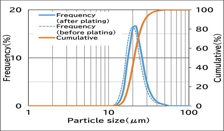
Proterial Metals has been developing and manufacturing conductive Ni-P particles as bonding materials. These Ni-P particles can be produced at particle sizes in the range of 1–30 μm, and are characterized by heat resistance, uniform particle size (see figure), high sphericity, and high hardness. While Proterial had held gold (Au) plated products to meet needs for high corrosion resistance as plating products until now, they were limited in achieving low electrical resistance. In response to this, Proterial Metals has developed a new plating technology that can plate Ni-P particles with materials other than Au.
With this technology, it is now possible to perform silver (Ag) plating and copper (Cu) plating—with low electrical resistance values—on conductive Ni-P particles. Volume resistivity in comparison with Au-plated Ni-P particles is around 1/5 for Ag plating and around 1/9 for Cu plating (see table). This has made it possible to support even higher speeds and capacities for signal transmission in electrical circuits. It also makes it possible to perform low-melting-point solder plating, which makes it possible to expand the contact area by soldering and reduce electrical resistance by metal bonding.
Because the heat resistance, uniform particle size (see figure) and sphericity that are characteristics of conventional Ni-P particles are maintained when applying these plating solutions, it is possible to maintain the flatness of the connection surface and the formation of appropriate gaps at the same level as conventional Ni-P particles. Since the core consists of Ni-P particles with high hardness, these plated particles are expected to be useful for bonding / mounting semiconductor chips to substrates such as silicon or glass.
Going forward, Proterial Metals will continue to contribute to improving the functional performance and lowering power consumption of semiconductors and related products using plated Ni-P particles with these characteristics.
3.Patents
Four patents pending for plating technologies
4.Production
Proterial Metals, Ltd. Kagoshima Works

Center: no plating. Left: silver plating. Top: gold plating. Bottom: copper plating. Right: solder plating.
| Types of plating | None | Au | Ag | Cu | Sn-Bi |
|---|---|---|---|---|---|
| Volume resistivity (x10-5 Ω・m)*1 | 21.1 | 0.6 | 0.13 | 0.07 | 0.5*2 |
| Melting point (ºC) | - | - | - | - | ≈160 |
- *1Volume resistivity varies depending on particle size, plating film thickness, and bonding state.
- *2The volume resistivity for solder is the value before soldering.
End
- Media Inquiries: Corporate Communications Dept.
https://www.cntct.proterial.com/contact/publish/inquiry_eng?g=01&c=001-01 - Customer Inquiries:
https://www.cntct.proterial.com/contact/publish/inquiry_eng?g=01&c=005